Documente Tehnice (Imaginile sunt cu titlu informativ. Va rugam sa consultati specificatiile tehnice.)
Specificatii
Marca
Renesas ElectronicsProduct Type
Clock Buffer
Maximum Input Frequency
133MHz
Maximum Propagation Delay Time
350ps
Montare
Surface
Tip pachet
SOIC
Numar pini
8
Tensiune de alimentare minima
3V
Tensiune de alimentare maxima
4.6V
Temperatura minima de lucru
-40°C
Temperatura maxima de lucru
85°C
Lungime
5mm
Inaltime
1.75mm
Standards/Approvals
RoHS
Series
IDT2305
Automotive Standard
No
Detalii Produs
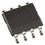
The Renesas Electronics high-speed phase-lock loop clock buffer, designed to address high-speed clock distribution applications. The zero delay is achieved by aligning the phase between the incoming clock and the output clock, operable within the range of 10 to 133MHz. It is an 8-pin version of the accepts one reference input, and drives out five low skew clocks.

Inspiră. Proiectează. Colaborează
ÎNSCRIE-TE GRATIS
Fara taxe ascunse!


Informatii despre stoc temporar indisponibile
€ 5,50
€ 0,55 Buc. (Intr-un pachet de 10) (fara TVA)
€ 6,66
€ 0,666 Buc. (Intr-un pachet de 10) (cu TVA)
Standard
10
€ 5,50
€ 0,55 Buc. (Intr-un pachet de 10) (fara TVA)
€ 6,66
€ 0,666 Buc. (Intr-un pachet de 10) (cu TVA)
Informatii despre stoc temporar indisponibile
Standard
10
| Cantitate | Pret unitar | Per Pachet |
|---|---|---|
| 10 - 10 | € 0,55 | € 5,50 |
| 20 - 40 | € 0,53 | € 5,30 |
| 50 - 90 | € 0,51 | € 5,10 |
| 100 - 280 | € 0,41 | € 4,10 |
| 290+ | € 0,40 | € 4,00 |
Inspiră. Proiectează. Colaborează
ÎNSCRIE-TE GRATIS
Fara taxe ascunse!
Documente Tehnice (Imaginile sunt cu titlu informativ. Va rugam sa consultati specificatiile tehnice.)
Specificatii
Marca
Renesas ElectronicsProduct Type
Clock Buffer
Maximum Input Frequency
133MHz
Maximum Propagation Delay Time
350ps
Montare
Surface
Tip pachet
SOIC
Numar pini
8
Tensiune de alimentare minima
3V
Tensiune de alimentare maxima
4.6V
Temperatura minima de lucru
-40°C
Temperatura maxima de lucru
85°C
Lungime
5mm
Inaltime
1.75mm
Standards/Approvals
RoHS
Series
IDT2305
Automotive Standard
No
Detalii Produs
The Renesas Electronics high-speed phase-lock loop clock buffer, designed to address high-speed clock distribution applications. The zero delay is achieved by aligning the phase between the incoming clock and the output clock, operable within the range of 10 to 133MHz. It is an 8-pin version of the accepts one reference input, and drives out five low skew clocks.
Inspiră. Proiectează. Colaborează
ÎNSCRIE-TE GRATIS
Fara taxe ascunse!