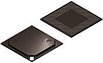
Documente Tehnice (Imaginile sunt cu titlu informativ. Va rugam sa consultati specificatiile tehnice.)
Specificatii
Marca
AlteraProduct Type
FPGA
Series
Cyclone IV E
Number of Logic Gates
6272
Number of Logic Cells
6272
Number of Logic Units
392
Number of Multipliers
360 (18 x 18)
Montare
Surface
Tensiune de alimentare minima
970mV
Tip pachet
FBGA
Numar pini
256
Tensiune de alimentare maxima
1.03V
Number of RAM Bits
276480bit
Temperatura minima de lucru
0°C
Temperatura maxima de lucru
85°C
Lungime
17mm
Standards/Approvals
No
Automotive Standard
No
Tara de origine
United States
Detalii Produs
An FPGA is a semiconductor device consisting of a Matrix of Configurable Logic Blocks (CLBs) connected through programmable interconnects. The user determines these interconnections by programming SRAM. A CLB can be simple (AND, OR gates, etc) or complex (a Block of RAM). The FPGA allows changes to be MADE to a design even after the device is soldered into a PCB.

Inspiră. Proiectează. Colaborează
ÎNSCRIE-TE GRATIS
Fara taxe ascunse!


Informatii despre stoc temporar indisponibile
€ 2.466,00
€ 27,40 Each (In a Tray of 90) (fara TVA)
€ 2.983,86
€ 33,154 Each (In a Tray of 90) (cu TVA)
90
€ 2.466,00
€ 27,40 Each (In a Tray of 90) (fara TVA)
€ 2.983,86
€ 33,154 Each (In a Tray of 90) (cu TVA)
Informatii despre stoc temporar indisponibile
90
Inspiră. Proiectează. Colaborează
ÎNSCRIE-TE GRATIS
Fara taxe ascunse!
Documente Tehnice (Imaginile sunt cu titlu informativ. Va rugam sa consultati specificatiile tehnice.)
Specificatii
Marca
AlteraProduct Type
FPGA
Series
Cyclone IV E
Number of Logic Gates
6272
Number of Logic Cells
6272
Number of Logic Units
392
Number of Multipliers
360 (18 x 18)
Montare
Surface
Tensiune de alimentare minima
970mV
Tip pachet
FBGA
Numar pini
256
Tensiune de alimentare maxima
1.03V
Number of RAM Bits
276480bit
Temperatura minima de lucru
0°C
Temperatura maxima de lucru
85°C
Lungime
17mm
Standards/Approvals
No
Automotive Standard
No
Tara de origine
United States
Detalii Produs
An FPGA is a semiconductor device consisting of a Matrix of Configurable Logic Blocks (CLBs) connected through programmable interconnects. The user determines these interconnections by programming SRAM. A CLB can be simple (AND, OR gates, etc) or complex (a Block of RAM). The FPGA allows changes to be MADE to a design even after the device is soldered into a PCB.
Inspiră. Proiectează. Colaborează
ÎNSCRIE-TE GRATIS
Fara taxe ascunse!