Documente Tehnice (Imaginile sunt cu titlu informativ. Va rugam sa consultati specificatiile tehnice.)
Specificatii
Marca
Renesas ElectronicsNumber of Drivers
2
Product Type
LVDS Buffer
Input Type
TTL
Sub Type
Buffer
Tip iesire
Buffer
Number of Elements per Chip
2
Montare
Surface
Tip pachet
TSSOP
Numar pini
20
Tensiune de alimentare minima
3V
Tensiune de alimentare maxima
3.3V
Frecventa minima de auto-rezonanta
-40°C
ESD Protection
Yes
Temperatura maxima de lucru
85°C
Lungime
6.6mm
Inaltime
1.05mm
Standards/Approvals
No
Series
9DB102
Automotive Standard
No
Detalii Produs
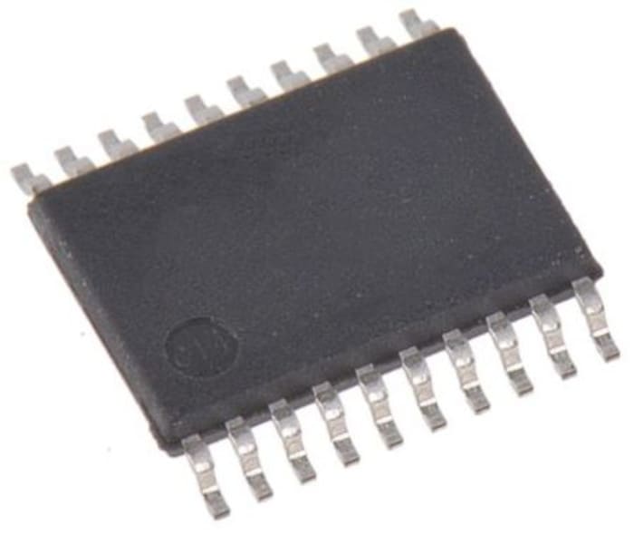
The Renesas Electronics 9DB102 zero-delay buffer supports PCI Express clocking requirements. The 9DB102 is driven by a differential SRC output pair from an IDT CK409/CK410-compliant main clock generator such as the 952601 or 954101. It attenuates jitter on the input clock and has a selectable PLL Band Width to maximize performance in systems with or without Spread- Spectrum clocking.

Inspiră. Proiectează. Colaborează
ÎNSCRIE-TE GRATIS
Fara taxe ascunse!


Informatii despre stoc temporar indisponibile
€ 189,44
€ 2,56 Each (In a Tube of 74) (fara TVA)
€ 229,22
€ 3,098 Each (In a Tube of 74) (cu TVA)
74
€ 189,44
€ 2,56 Each (In a Tube of 74) (fara TVA)
€ 229,22
€ 3,098 Each (In a Tube of 74) (cu TVA)
Informatii despre stoc temporar indisponibile
74
Inspiră. Proiectează. Colaborează
ÎNSCRIE-TE GRATIS
Fara taxe ascunse!
Documente Tehnice (Imaginile sunt cu titlu informativ. Va rugam sa consultati specificatiile tehnice.)
Specificatii
Marca
Renesas ElectronicsNumber of Drivers
2
Product Type
LVDS Buffer
Input Type
TTL
Sub Type
Buffer
Tip iesire
Buffer
Number of Elements per Chip
2
Montare
Surface
Tip pachet
TSSOP
Numar pini
20
Tensiune de alimentare minima
3V
Tensiune de alimentare maxima
3.3V
Frecventa minima de auto-rezonanta
-40°C
ESD Protection
Yes
Temperatura maxima de lucru
85°C
Lungime
6.6mm
Inaltime
1.05mm
Standards/Approvals
No
Series
9DB102
Automotive Standard
No
Detalii Produs
The Renesas Electronics 9DB102 zero-delay buffer supports PCI Express clocking requirements. The 9DB102 is driven by a differential SRC output pair from an IDT CK409/CK410-compliant main clock generator such as the 952601 or 954101. It attenuates jitter on the input clock and has a selectable PLL Band Width to maximize performance in systems with or without Spread- Spectrum clocking.
Inspiră. Proiectează. Colaborează
ÎNSCRIE-TE GRATIS
Fara taxe ascunse!