Documente Tehnice (Imaginile sunt cu titlu informativ. Va rugam sa consultati specificatiile tehnice.)
Specificatii
Marca
Renesas ElectronicsProduct Type
Clock Buffer
Montare
Surface
Tip pachet
TSSOP
Tensiune de alimentare minima
1.5V
Numar pini
16
Tensiune de alimentare maxima
3.3V
Temperatura minima de lucru
0°C
Temperatura maxima de lucru
70°C
Lungime
4mm
Inaltime
0.9mm
Standards/Approvals
No
Series
8305A
Automotive Standard
No
Detalii Produs
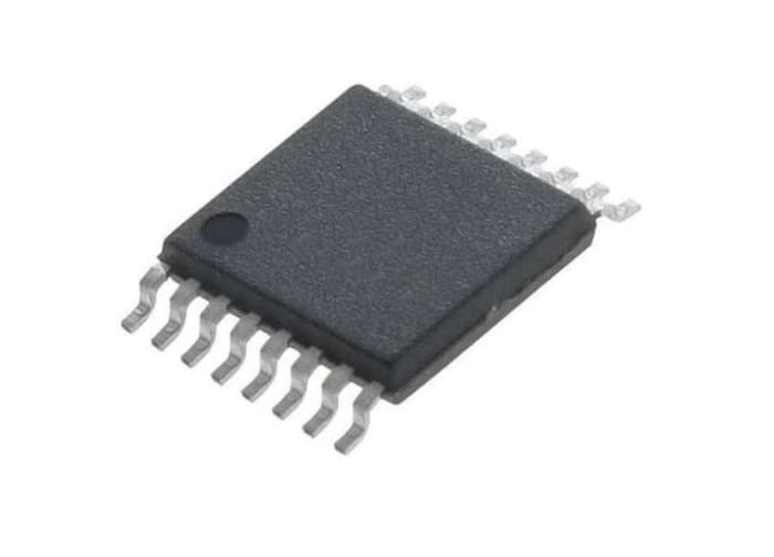
The Renesas Electronics ICS8305 is a low skew, 1-to-4, Differential/ LVCMOS-to-LVCMOS/LVTTL Fanout Buffer. The ICS8305 has selectable clock inputs that accept either differential or single ended input levels. The clock enable is internally synchronized to eliminate runt pulses on the outputs during asynchronous assertion/deassertion of the clock enable pin. Outputs are forced LOW when the clock is disabled. A separate output enable pin controls whether the outputs are in the active or high impedance state.

Inspiră. Proiectează. Colaborează
ÎNSCRIE-TE GRATIS
Fara taxe ascunse!


Informatii despre stoc temporar indisponibile
€ 353,28
€ 3,68 Each (In a Tube of 96) (fara TVA)
€ 427,47
€ 4,453 Each (In a Tube of 96) (cu TVA)
96
€ 353,28
€ 3,68 Each (In a Tube of 96) (fara TVA)
€ 427,47
€ 4,453 Each (In a Tube of 96) (cu TVA)
Informatii despre stoc temporar indisponibile
96
Inspiră. Proiectează. Colaborează
ÎNSCRIE-TE GRATIS
Fara taxe ascunse!
Documente Tehnice (Imaginile sunt cu titlu informativ. Va rugam sa consultati specificatiile tehnice.)
Specificatii
Marca
Renesas ElectronicsProduct Type
Clock Buffer
Montare
Surface
Tip pachet
TSSOP
Tensiune de alimentare minima
1.5V
Numar pini
16
Tensiune de alimentare maxima
3.3V
Temperatura minima de lucru
0°C
Temperatura maxima de lucru
70°C
Lungime
4mm
Inaltime
0.9mm
Standards/Approvals
No
Series
8305A
Automotive Standard
No
Detalii Produs
The Renesas Electronics ICS8305 is a low skew, 1-to-4, Differential/ LVCMOS-to-LVCMOS/LVTTL Fanout Buffer. The ICS8305 has selectable clock inputs that accept either differential or single ended input levels. The clock enable is internally synchronized to eliminate runt pulses on the outputs during asynchronous assertion/deassertion of the clock enable pin. Outputs are forced LOW when the clock is disabled. A separate output enable pin controls whether the outputs are in the active or high impedance state.
Inspiră. Proiectează. Colaborează
ÎNSCRIE-TE GRATIS
Fara taxe ascunse!