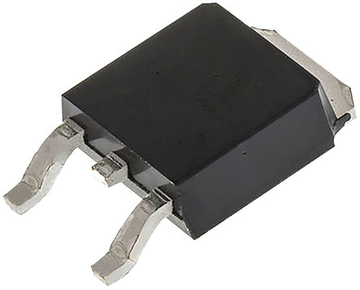
onsemi P-Channel MOSFET, 5.7 A, 200 V, 3-Pin DPAK FQD7P20TM

Documente tehnice (Imaginile sunt cu titlu informativ. Va rugam sa consultati specificatiile tehnice.)
Specificatii
Marca
onsemiChannel Type
P
Maximum Continuous Drain Current
5.7 A
Maximum Drain Source Voltage
200 V
Tip pachet
DPAK (TO-252)
Timp montare
Surface Mount
Numar pini
3
Maximum Drain Source Resistance
690 mΩ
Channel Mode
Enhancement
Minimum Gate Threshold Voltage
3V
Maximum Power Dissipation
55 W
Transistor Configuration
Single
Maximum Gate Source Voltage
-30 V, +30 V
Latime
6.22mm
Transistor Material
Si
Number of Elements per Chip
1
Lungime
6.73mm
Typical Gate Charge @ Vgs
19 nC @ 10 V
Temperatura maxima de lucru
+150 °C
Inaltime
2.39mm
Temperatura minima de lucru
-55 °C
Detalii produs
Enhancement Mode P-Channel MOSFET, ON Semiconductor
ON Semiconductors range of P-Channel MOSFETS are produced using ON Semi’s proprietary, high cell density, DMOS technology. This very high density process has been designed to minimize on-state resistance to provide a rugged and reliable performance for fast switching.
MOSFET Transistors, ON Semi
ON Semi offers a substantial portfolio of MOSFET devices that includes high-voltage (>250V) and low-voltage (<250V) types. The advanced silicon technology provides smaller die sizes, which it is incorporated into multiple industry-standard and thermally-enhanced packages.
ON Semi MOSFETs provide superior design reliability from reduced voltage spikes and overshoot, to lower junction capacitance and reverse recovery charge, to elimination of additional external components to keep systems up and running longer.
Inspiră. Proiectează. Colaborează
ÎNSCRIE-TE GRATIS
Fara taxe ascunse!


- Descărcați și utilizați software-ul nostru DesignSpark pentru modelele dumneavoastră PCB și mecanice 3D
- Vizualizați și contribuiți cu conținutul site-ului web și forumuri
- Descărcați modele 3D, scheme și amprente de la peste un milion de produse
€ 1.150,00
€ 0,46 Buc. (Pe o rola de 2500) (fara TVA)
€ 1.391,50
€ 0,557 Buc. (Pe o rola de 2500) (cu TVA)
2500
€ 1.150,00
€ 0,46 Buc. (Pe o rola de 2500) (fara TVA)
€ 1.391,50
€ 0,557 Buc. (Pe o rola de 2500) (cu TVA)
Informatii despre stoc temporar indisponibile
2500
Informatii despre stoc temporar indisponibile
Inspiră. Proiectează. Colaborează
ÎNSCRIE-TE GRATIS
Fara taxe ascunse!
- Descărcați și utilizați software-ul nostru DesignSpark pentru modelele dumneavoastră PCB și mecanice 3D
- Vizualizați și contribuiți cu conținutul site-ului web și forumuri
- Descărcați modele 3D, scheme și amprente de la peste un milion de produse
Documente tehnice (Imaginile sunt cu titlu informativ. Va rugam sa consultati specificatiile tehnice.)
Specificatii
Marca
onsemiChannel Type
P
Maximum Continuous Drain Current
5.7 A
Maximum Drain Source Voltage
200 V
Tip pachet
DPAK (TO-252)
Timp montare
Surface Mount
Numar pini
3
Maximum Drain Source Resistance
690 mΩ
Channel Mode
Enhancement
Minimum Gate Threshold Voltage
3V
Maximum Power Dissipation
55 W
Transistor Configuration
Single
Maximum Gate Source Voltage
-30 V, +30 V
Latime
6.22mm
Transistor Material
Si
Number of Elements per Chip
1
Lungime
6.73mm
Typical Gate Charge @ Vgs
19 nC @ 10 V
Temperatura maxima de lucru
+150 °C
Inaltime
2.39mm
Temperatura minima de lucru
-55 °C
Detalii produs
Enhancement Mode P-Channel MOSFET, ON Semiconductor
ON Semiconductors range of P-Channel MOSFETS are produced using ON Semi’s proprietary, high cell density, DMOS technology. This very high density process has been designed to minimize on-state resistance to provide a rugged and reliable performance for fast switching.
MOSFET Transistors, ON Semi
ON Semi offers a substantial portfolio of MOSFET devices that includes high-voltage (>250V) and low-voltage (<250V) types. The advanced silicon technology provides smaller die sizes, which it is incorporated into multiple industry-standard and thermally-enhanced packages.
ON Semi MOSFETs provide superior design reliability from reduced voltage spikes and overshoot, to lower junction capacitance and reverse recovery charge, to elimination of additional external components to keep systems up and running longer.
Inspiră. Proiectează. Colaborează
ÎNSCRIE-TE GRATIS
Fara taxe ascunse!
- Descărcați și utilizați software-ul nostru DesignSpark pentru modelele dumneavoastră PCB și mecanice 3D
- Vizualizați și contribuiți cu conținutul site-ului web și forumuri
- Descărcați modele 3D, scheme și amprente de la peste un milion de produse